TM9-4935-481-14-1
the inputs. This protects the input transistor and reduces the ringing at the inputs. The undesirable ringing is peculiar to TTL
logic and is associated with its very fast switching times.
d. Gates and Their Functions.
(1) General. AND, NAND, OR and NOR gates may have any number of inputs, but only one output. An inverter has
only one input and one output.
(2) AND gate (MIS-18698/106-01). The output is high only if all inputs are high (therefore if one or more of the
inputs are low the output is low) (fig. 3-10).
(3) Inverter (MIS-18698/113-01). The output is opposite to the input. Therefore if the input is low the output is high,
and if the input is high, the output is low (fig. 3-11).
(4) NAND gate (MIS-18698/120-01, MIS-18698/101-01, MIS-18698/008-01-Z, MIS-18698/028-01-Z, MIS-18698/115-
01, MIS-18698/116-01). The output is low only if all inputs are high (therefore, the output is high if one or more inputs are
low) (fig. 3-12).
(5) OR gate (MIS-18698/104-01). The output is low only if all inputs are low (therefore, if one or more inputs are
high, the output is high) (fig. 3-13).
(6) NOR gate (MIS-18698/103-01). The output is high only if all inputs are low (therefore, if one or more inputs are
high, the output is low) (fig. 3-14).
(7) Expandable NAND gates (MIS-18698/101-01 and MIS-18698/008-01Z). The circuit shown in figure 3-15 will
delay the high-to-low transition of the output from the time all inputs became high. The amount of time delay is given by an
approximate formula: TD 30 +1.4C, where TD is time delay in nSEC, C is capacitance in pfd. The amount of delay
changes with temperature and power supply voltage, therefore, this type of delay is used only where large tolerances (in the
order of 50%) of the time delay are permissible.
(8) Wired AND connection. Figure 3-16 shows several methods used for wiring the outputs of various logic
elements. From figure 3-16 it is seen that the connection of two or more outputs may be replaced by (is equivalent to) and
AND gate. The wired AND connection can be used only with the outputs of those gates which do not use transistor or other
active devices in its output to "pull" that output high. Diode-Transistor Logic (DTL), with the exception of some buffers, use
resistors as output pull-up elements. Therefore, those DTL outputs, with resistors as the output pull-up, can be wired AND.
Transistor-Transistor Logic (TTL) use transistors as output pull-up elements (with the exception of "open collector" outputs).
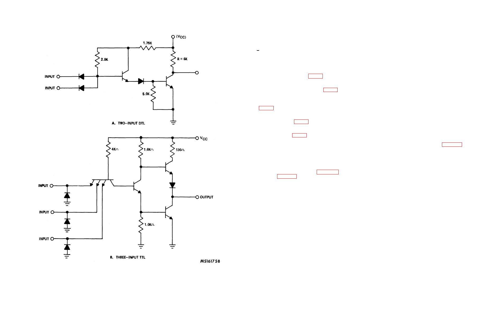
Figure 3-9. NAND gate schematics
3-18


