
TM9-4935-481-14-1
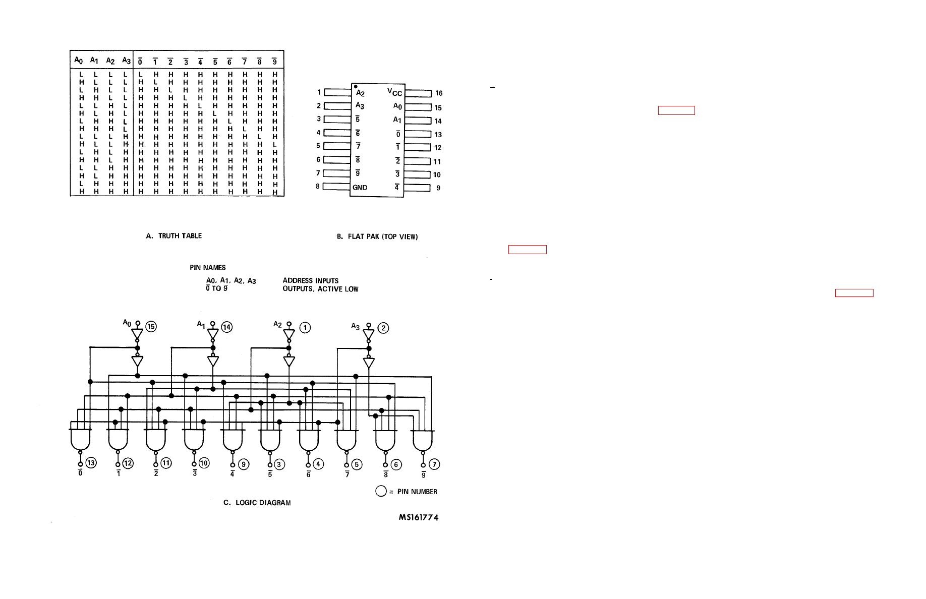
exclusive active LOW outputs, as shown by the logic symbol. The active LOW outputs facilitate addressing other logic
elements with active LOW enables. The logic design of the decoder ensures that all outputs are HIGH when binary codes
greater than nine are applied to the inputs.
h. Differentiating Circuit Driving a Gate.
(1) Circuit requirements. When it is required to generate a short low level logic pulse coincident with the high-to-low
transition of a given digital signal, the circuit shown in figure 3-26 is used.
(2) Circuit inputs. When the input to this circuit is high (typically +3.5 Vdc), the output is half of +5 Vdc, or +2.5 Vdc,
which is logic high. The voltage (Vc) across the capacitor (C) is +2.5 Vdc -3.5 = -1 Vdc. If the voltage at the input changes
from +3.5 Vdc to +0.2 Vdc (logic low) the capacitor holds its initial charge at the instant of the transition. Therefore, the
voltage across the capacitor is -1 Vdc at that instant. The output voltage (Vo) is equal to the input voltage (Vin) plus the
capacitor voltage (Vc).
or Vo = Vin + Vc
Vo = +.2 Vdc + (-1 Vdc)
Vo = -.8 Vdc
As the capacitor charges exponentially to its new steady state voltage which is +2.5 Vdc -0.2 Vdc = +2.3 Vdc, the output
voltage increases until it reaches +2.5 Vdc.
(3) Circuit outputs. When the output is below +0.4V, it is equivalent to a digital low. The duration of this low
depends on the value of the capacitor C1. Larger values of C give longer low pulse. When the input to the circuit is a low-to-
high transition, the output will step from +2.5 Vdc to approximately +4.8 Vdc, and then exponentially decrease to +2.5 Vdc as
shown in figure 3-26,B. The gate connected to the output sees a continuous high because the output does not fall below +2.4
Vdc.
i.
Switch/Digital-Input Interfaces.
(1) Circuit requirements. The interface of a single pole on-off switch to digital input is shown in figure 3-27. When
the switch is in the position shown, the output of this circuit (input to digital circuit) is LOW (O Vdc). When the switch is in the
opposite position, the resistor R1 pulls the line up to approximately +5 Vdc (HIGH). The value of RI is not critical, and may
be from 120 ohms to 10K. Low values of R1 cause higher power dissipation in the LOW state, but
Figure 3-25. One-in-ten decoder
3-27
