
TM9-4935-481-14-1
C1
Both inputs (pin 2 and 3) must be high to turn the lamp ON. When the lamp driver is ON, the voltage at the output is
provide better immunity for capacitively or inductively coupled noise in the HIGH state. A typical value for R1, which is a
compromise between high power dissipation and good noise immunity, is 5.1K.. This circuit generates a short burst of noise
approximately one volt less than the voltage at pin 1. When the lamp driver is OFF, the output voltage is approximately 0
Vdc.
pulses every time S1 is switched ON or OFF due to the contact bounce of the switch. When the digital input requires clean
transition from one state to another, the above circuit cannot be used, and a debouncing circuit (figure 3-28) must be used.
(2) Debouncing. This circuit (fig. 3-28) consists of an ON-ON switch, two pull-up resistors and an R-S flip-flop.
When switch S1 is in the position shown, the Q output is HIGH, and the Q output is LOW (R-S flip-flop is in SET state).
When S1 is being switched to the opposite position, and the pole of the switch is traveling between the two contacts, the
outputs remain in their original states, but change to opposite states as soon as the pole touches the lower contact. The Q
output is now LOW, and the Q output is HIGH (the R-S flip-flop is now in RESET state). Due to the latching action of the flip-
flop, the outputs remain in these states after the pole bounces from the lower contact, provided the pole does not bounce all
the way back to the upper contact. When S1 is switched again, so that the pole travels toward the upper contact, the outputs
remain unchanged until the pole touches the upper contact, causing the outputs to change state. The Q output is now HIGH,
and Q output is LOW (flip-flop is in SET state). Due to the latching action of the R-S flip-flop, the outputs remain in these
states after the pole bounces from the upper contact, provided it does not bounce all the way back to the lower contact.
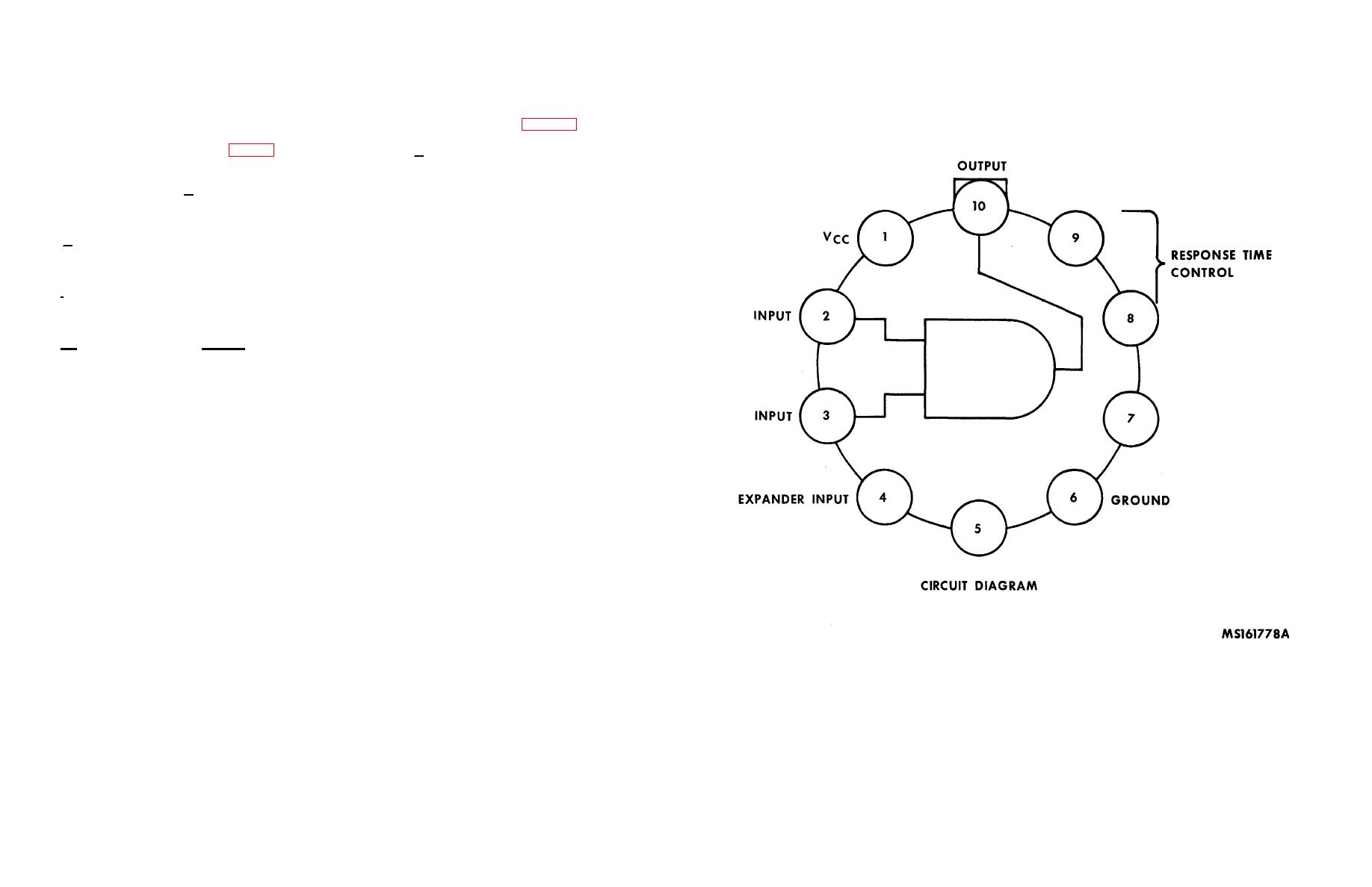
j. TTL or DTL to Lamp Interface-Lampdriver. (MIS-18698/072-01-Z) The TTL and DTL outputs have low output
currents and cannot drive high intensity incandescent lamps directly, but require special lamp drivers. The pin functions of
the lamp drivers used in DMS are listed below:
Pin
Function
1
+24 Vdc power input
2
Control signal input
3
Control signal input
4
Expander input
6
+24 Vdc return, and control signal return
8, 9
Output voltage slew rate control (capacitor)
10
Output (to lamp)
Figure 3-29. TTL or DTL to lamp interface - lampdriver
3-29
