TM9-4935-481-14-1
C2
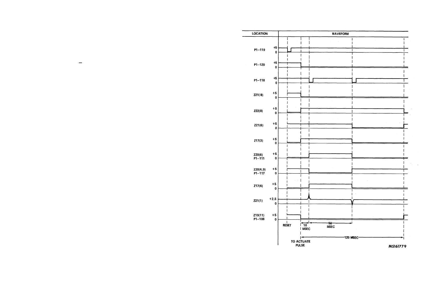
generator. Pin 6(Q) of Z20 switches to the "1" state and pin 9 (Q) switches to the "0" state. The output of Z17 (pin 6)
switches to the "1" state.
(h) The output of Z17 (pin 6) is connected to a differentiating circuit consisting of resistor R3 and capacitor C2.
The input to Z21 (pin 1) is a positive spike pulse which switches from the initial dc level of +2.5 Vdc to approximately +7.5V
peak. This pulse will not cause Z21 (pins 3 and 6) to switch states. Therefore Z20 is still enabled.
(i) Z20 is now triggered by the negative slope of the second pulse from the pulse generator (50 msec from the
negative slope of the first pulse). Pin 6 (Q) of Z20 now switches to the "0" state and pin 9 (Q) switches to the "1" state. The
output of Z17 (pin 6) switches to the "0" state.
(j) The input to Z21 (pin 1, which had stabilized to +2.5 Vdc) now is a negative spike pulse which switches from
the initial dc level of +2.5 Vdc to approximately -2.5 Vdc. This pulse will cause the output of Z21 (pin 6) to switch to the "0"
state. The output of Z17 (pin 3) now switches to the "0" state, disabling Z20.
(k) The output of Z22 switches from the "1" state to the "0" state 146 msec (nominal) from Ts. The outputs of
Z21 (pin 6) and Z19 switch to the "1" state. The output of Z17 (pin 3) remains in the "0" state since the input to Z17 (pin 2) is
a "0". The resultant waveforms will be shown in fig. 4-46.
NOTE
The waveforms shown in fig. 4-46 are system waveforms which are applicable to the
circuit performance when the assembly is installed in DMS-D, but which do not
necessarily apply to the circuit performance while tested in DMS-G.
Figure 3-30. Circuit card A7-waveforms
3-30.5


